
Precision process application

Microelectronics Laser Soldering

Microelectronics soldering often raises questions about small joint geometry, confined access and controlled heat input. Laser solder ball jetting combines ball delivery, localized laser heating, positioning and programmable motion into a process that can be evaluated for these conditions.

Application challenge

Start with the real assembly environment

The challenge is to create a repeatable process around the specific component design while avoiding broad claims that do not belong to the actual sample.

Joint geometry

Define the working envelope

Pad size, surface finish, clearance, joint shape, part flatness and position reference define the working envelope more reliably than a generic product category.

Microelectronics joint and pitch context

Application-specific engineering questions

Supplied process and sample evidence supports the reading experience without being presented as an undocumented customer project.

01

Geometry should lead the discussion

Microelectronic assemblies often make pad size, surface finish, clearance, access and fixture flatness central to the soldering question. A product category is not enough to select a process; the working envelope should be defined from the actual component and joint.
02

Use fine-pitch footage only as factual evidence

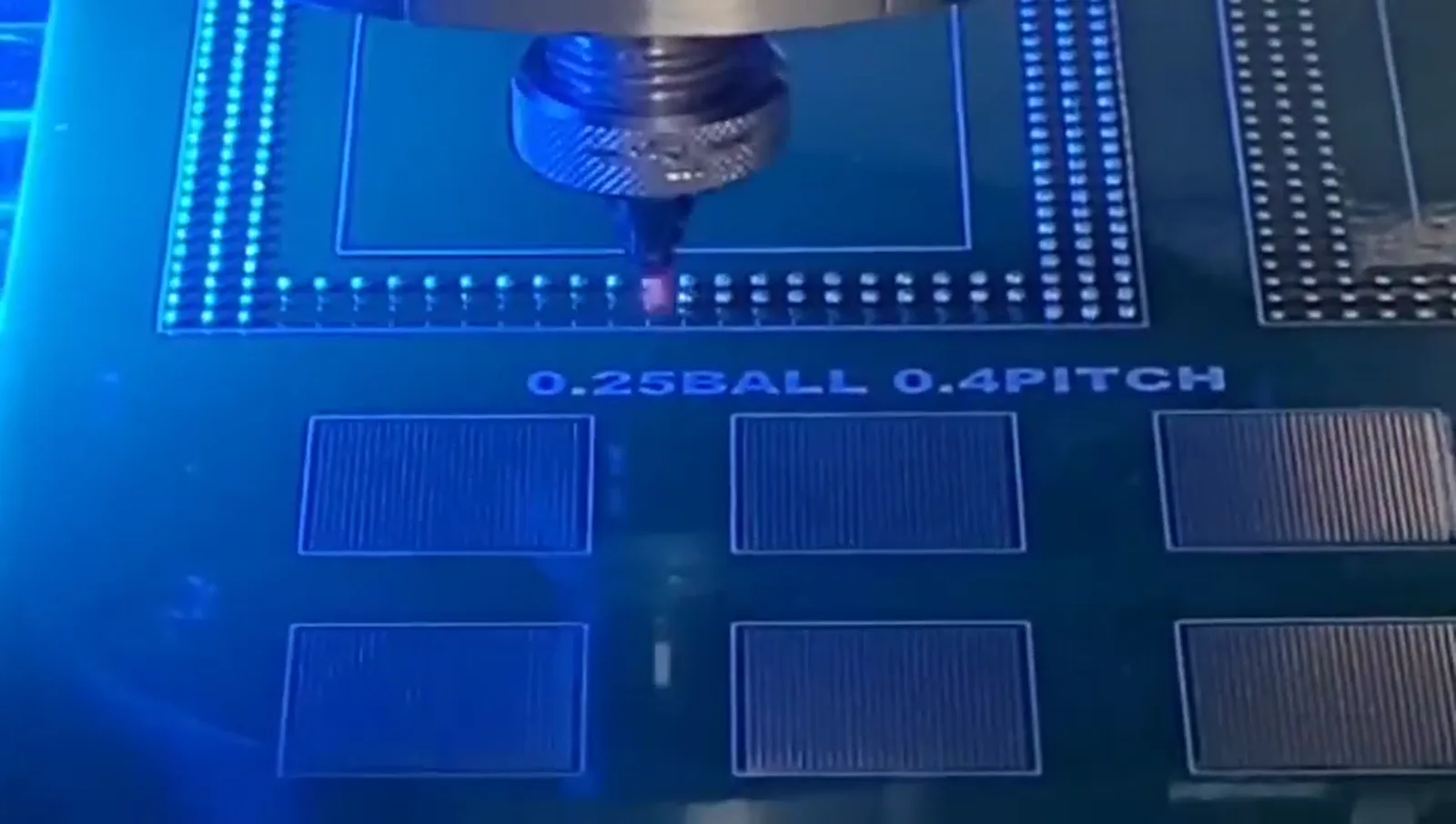
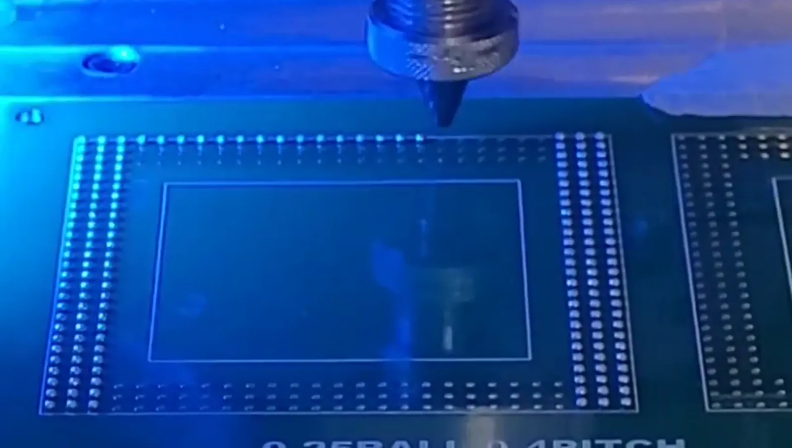
The supplied video includes a frame marked 0.25 BALL and 0.4 PITCH. It demonstrates 0.25 mm solder ball processing on a 0.4 mm pitch test pattern. It does not establish an unspecified minimum ball size, pitch or guaranteed performance on another design.

03

Positioning must include the entire reference chain

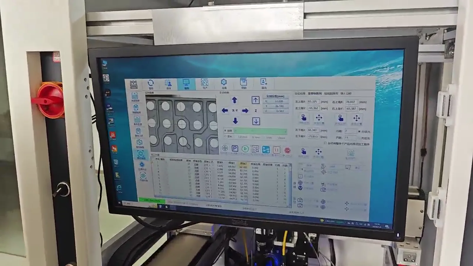
Vision, motion and a fixture can contribute to a precise relationship, but each depends on the other. The appropriate discussion includes the part datum, the image feature where used, the workholding repeatability and the nozzle-to-pad access path.

What matters in evaluation

Process considerations for Microelectronics

A feasibility review makes part-specific constraints explicit before automation is selected.

01

Solder-ball diameter and joint-geometry review

02

Vision or datum-based positioning

03

Fixture and access analysis

04

Sample inspection after controlled trials

Configuration path

Choose the system after the process

The fine-pitch demonstration material is a useful process visual: it demonstrates 0.25 mm solder ball processing on a 0.4 mm pitch test pattern, not a universal minimum specification.

Explore custom automation

How to test

Prepare a useful sample evaluation

Send samples, close-up photographs, pad data, acceptance criteria and expected process volume for an engineering review.

View sample-testing process

Supplied sample evidence

Local processing, visible sample context

Sample photography supports technical discussion without attributing imagery to an undocumented customer or claiming mass-production results.

Real supplied sample imagery

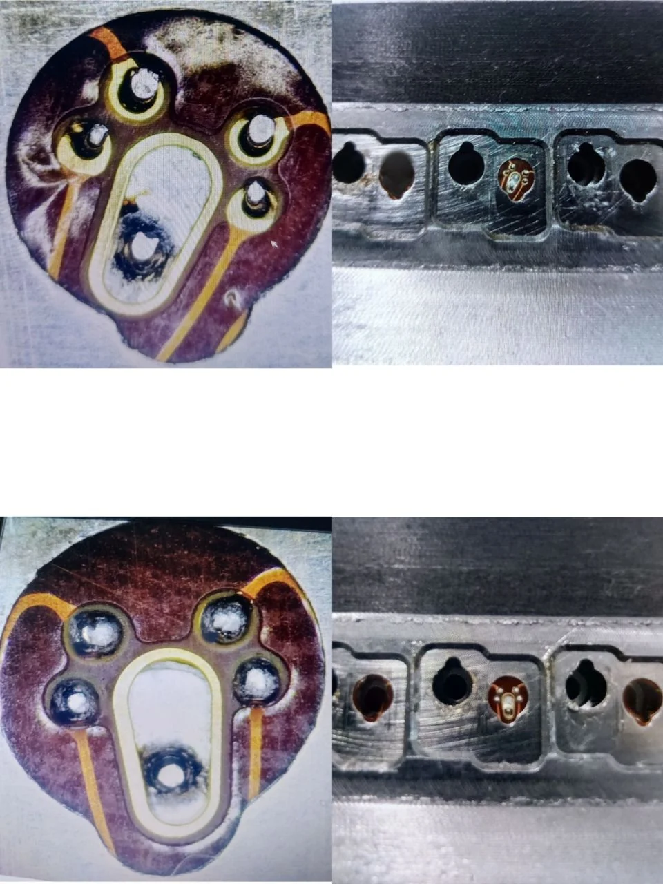
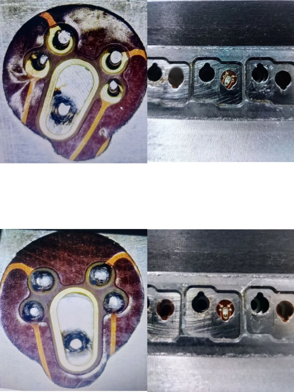
Sample solder joint before / after processing

Before / After
Sample solder joint before laser solder ball processing
Before soldering
Sample solder joint after laser solder ball processing
After laser solder ball processing

Real supplied images; visible appearance should be judged against the requirement for the actual component.

Have a micro-soldering application to evaluate?

Send the component information. Start with the process.

Share drawings, sample photographs or soldering requirements. The engineering discussion can connect the component to a suitable process and machine configuration.

WhatsApp Email