
Potential optoelectronic application
Optoelectronic Component Soldering
Optoelectronic assemblies may contain light-sensitive, heat-sensitive or alignment-sensitive elements near the target joint. Laser solder ball jetting can be evaluated for its localized process approach, while the overall component risk must be defined by the application owner.
Application challenge
Start with the real assembly environment
The target joint must be approached with an understanding of optical surfaces, package materials, fixture protection and any restrictions around local heating.
Joint geometry
Define the working envelope
Application information should clarify the solder location, nearby functional elements, clearance, part orientation and any keep-out zones.
What matters in evaluation
Process considerations for Optoelectronics
A feasibility review makes part-specific constraints explicit before automation is selected.
Datum strategy that respects alignment requirements
Controlled solder-volume evaluation
Trial review using customer-defined criteria
Configuration path
Choose the system after the process
A guarded fixture and careful positioning concept may be more important than a particular base-machine format.
Explore custom automationHow to test
Prepare a useful sample evaluation
Supply component images, technical drawings if available, material/keep-out notes and preferred joint sequence.
View sample-testing processSupplied sample evidence
Local processing, visible sample context
Sample photography supports technical discussion without attributing imagery to an undocumented customer or claiming mass-production results.
Real supplied sample imagery
Sample solder joint before / after processing
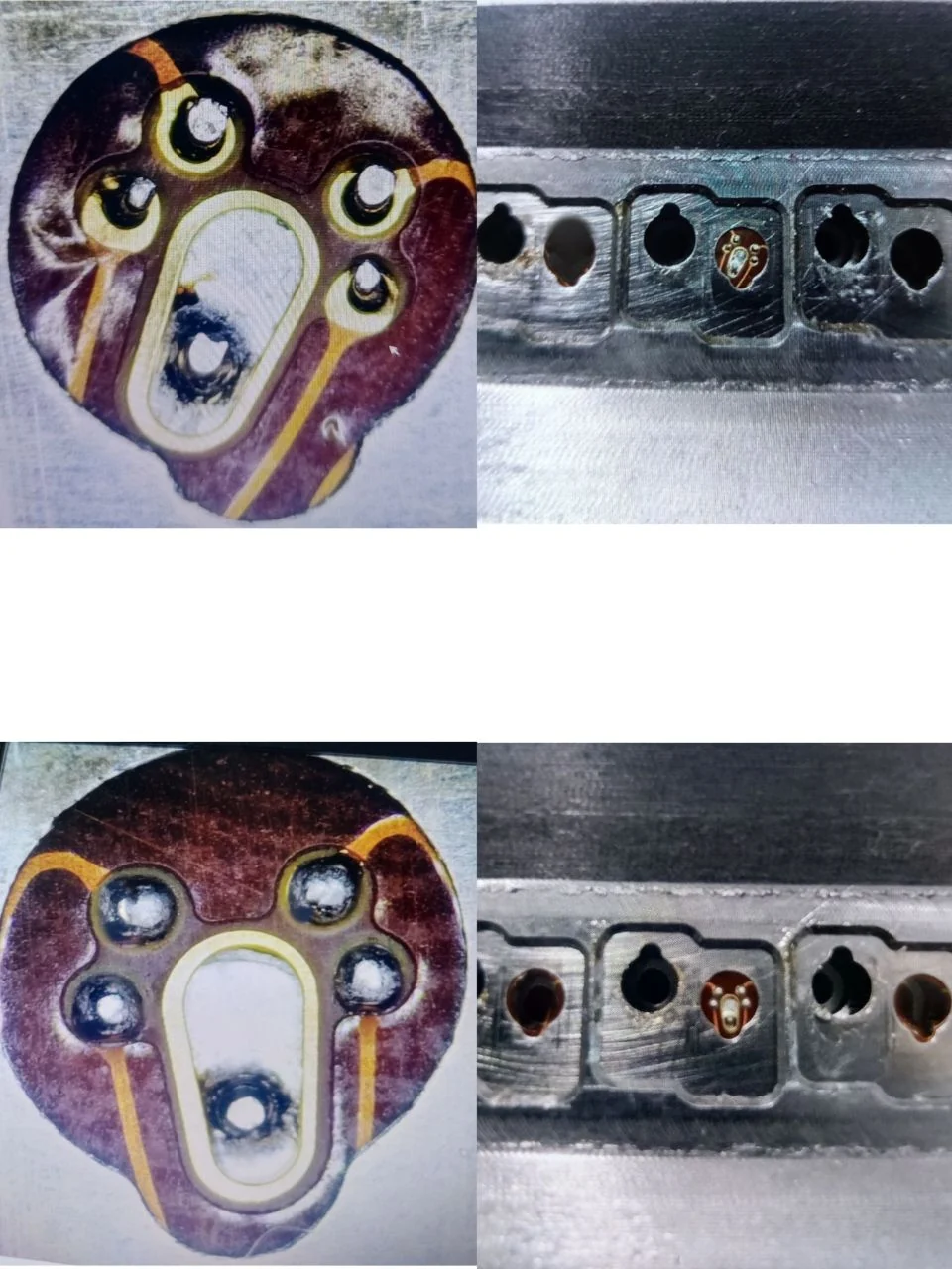
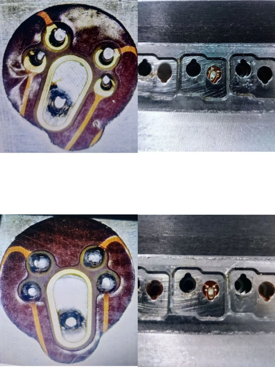
Real supplied images; visible appearance should be judged against the requirement for the actual component.
Related engineering paths
Continue with the information that matters next
Internal links are selected for application relevance rather than placed as an artificial SEO list.
Laser Solder Ball Jetting Machine
A configurable laser solder ball jetting system for localized soldering of small electronic joints.
Explore →Dual-Station Solder Ball Jetting System
A two-station concept for applications that benefit from separated operator, fixture, loading or processing tasks.
Explore →Inline Laser Solder Ball Jetting System
A laser solder ball jetting concept for integration into a defined inline manufacturing flow.
Explore →Have a micro-soldering application to evaluate?
Send the component information. Start with the process.
Share drawings, sample photographs or soldering requirements. The engineering discussion can connect the component to a suitable process and machine configuration.